
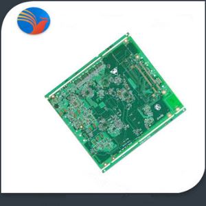


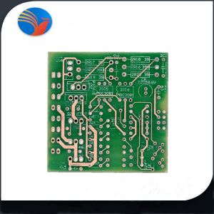
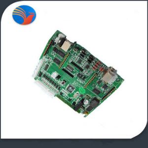
Home Automation Air Conditioner Universal Pcb Board
-
Payment


-
Origin
China Mainland
-
Minimum Order
5
-
Packing
Pieces
- Contact Now Start Order
- Description
Product Detail
Product Description
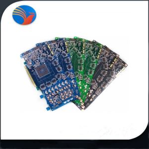
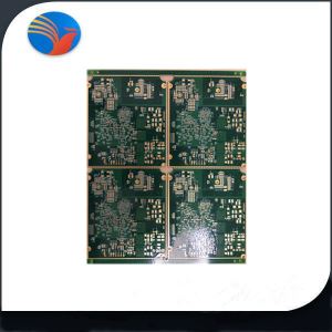
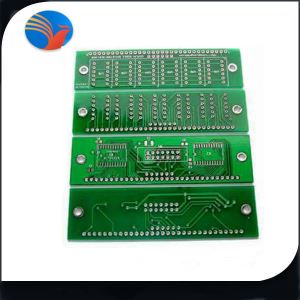
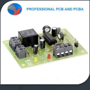
1. Products show :
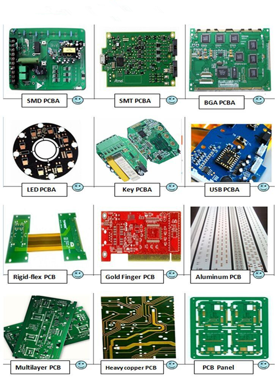
2. PCB ASSEMBLY CAPABILITY
Capability | Standard | Advanced |
Laminate materials | FR4 / FR1 / CEM-3 / CEM-1 / Aluminum / Rigid-Flex PCB/ Arlon / High-TG/ Rogers / Teflon / Taconic | |
Surface Finish | HASL (vertical & Horizontal), Lead Free HASL, HASL+Gold Finger, OSP/Entek, ENIG, ENEPIG, Immersion Tin(ISn) ,Immersion Silver(IAg), Carbon Ink, Hard Gold(Flash Gold), Soft Gold | |
Min. Thickness for inner layers | 0.020"-0.125" | 0.003”(0.07mm) |
Board layers | 1-24 Layers | 1-24 Layers |
Board Thickness | 0.1mm-3mm | 0.1mm-7mm |
Copper weight | 0.5 oz – 6 oz | 0.5 oz – 8 oz |
Minimum Trace Width / Spacing | 0.003"/0.003" | 0.003"/0.003" |
Solder Mask Color | Green,Blue,Black,Red,Yellow,White, and customized | |
Drill deviation | 0.004" | ±0.002” (0.05mm) |
PTH hole tolerance | 0.004" | ±0.002” (0.005mm) |
NPTH hole tolerance | 0.008" | ±0.002” (0.005mm) |
Min hole size | 0.004" | 0.008” (0.02mm) |
E-test | Flying Probe Tester/Test-Jig/X-ray/ICT/AOI/FCT | |
Controlled Tolerance | ±3% | ±3% |
Silkscreen Color | White, Black, Yellow, Green, Red, Blue and customized | |
Min solder mask clearance size | 0.008 | 0.003” (0.07mm) |
Min silkscreen clearance size | 0.010" | 0.006” (0.15mm) |
IPC Class | Class 2 | Class 3 |
Blind Vias | YES | YES |
Buried Vias | YES | YES |
Aspect Ratio | 8/1 | 15/1 |
Carbon Ink | YES | YES |
Peelable Mask | YES | YES |
Solder Sample | YES | YES |
First Article | YES | YES |
Certificate: | UL / SGS / ROH / ISO / TS16949 / ISO14001:2004 | |
Acceptable file format | GERBER file, PROTEL 99/PADS / POWER PCB / AutoCAD /EAGLE | |
Our Servise
1.Trade Assurance

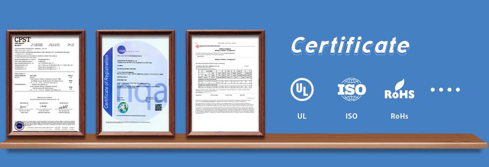
2. Certificate
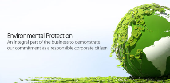
3. Environmental Protection Policy
Noeya’s highest priority is in the conservation and protection of the environment. The Company encourages all personnel to be environmentally conscious and acknowledges its responsibilities to undertake every possible action to prevent pollution, as required by National and International Rules and Regulations and legislation in force.
Why choose us ???
Professional on PCB & PCBA for 12 years -- One-Stop Service!!!!
1:PCB EMC design/corrective services/Testing sevices/Certification services
2:From 2 to 24 layers PCB Fabrication
3:From sample to batch processing
4:48 hours fastest delivery
5:IPC2/3 acceptance criteria
6:Factory direct wholesale price
7:Replying with price within 1 day.
Certificate: ROHS, UL,SGS,9001-2000, ISO14001, SGS Lead-Free
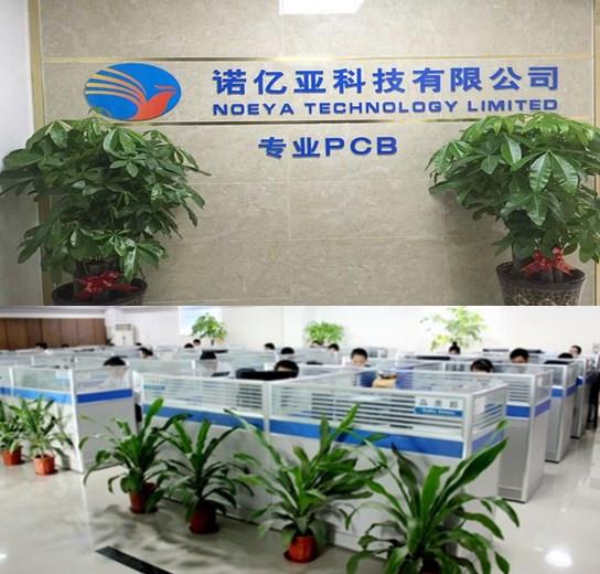
Company Information
WELCOME TO NOEYA PCB AND PCBA COMPANY
NOEYA TECHNOLOGY LTD founded in the year 2003, located in shenzhen, China. We are a professional EMS/OEM company; provide one-stop contract electronic manufacturing service for PCB&PCBA.
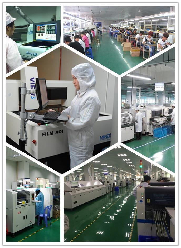
For assembly, utilizing 12 high-speed SMT lines from Yamaha and Sony, to meet customers' need.
Another, we are 6 years alibaba gold supplier and Trade Assurance Supplier to guarantee your benefit.
NOEYA covers an area of 10,000 square meters and can monthly yield 30,000~40,000square meters or more ,among which, 40% are exported to foreign countries.
Our Factory
1. Factory Information :
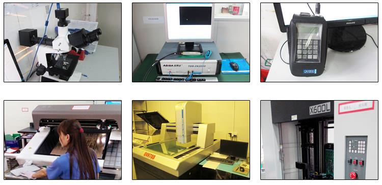
2. Test equipments
Packaging & Shipping
Packaging and Shipping

FAQ
1.Which type of PCB and PCBAs do you expert in?
We are specialized in producing HDI multilayer blind, BGA, impedance, half-hole, double-sided, single-sided, etc.
2.Quotation requirement for PCB and PCB Assembly ?
Gerber file and BOM list, clear pics of PCBA or PCBA sample for us, test method for PCBA.
3.What kind of PCB file format can you accept for production? What CAM software do you use?
We accept Gerber file for production. CAM350, GENESIS, UCAM, GC-CAM, V-2000.
4.Can you design gerber file?
We can design gerber file if customer can provide us schematic, schematic sample can also be provided if customer want.
5.I only have the pcb sample, not pcb file, can you produce it for me?
Yes, we can copy file based on your sample, this file names gerber, and production then is accorded to gerber file.
6.What is your minimum order quantity?
We have no limitation on MOQ, prototype, medium volume and large volume are all acceptable.
7.What is your produce ability?
Our ability is average 40,000 square meters per month.
8.Will you allow me to put several part number together into one panel?
Yes, this is usually happen in we factory, this way can help customers reduce some cost and to a certain degree, it can help reduce some assembly cost.
9.Are my design files safe when I submit them to you for manufacturing?
Any customer’s file will be protected very well here in our factory and we will not let any third party know. We can sign NDA with you.
Contact Us

![]()
![]()
![]()
![]()
pcb and pcb Assembly Manufacturer
-
Tablet Circuit Board Pcb Supplier 5 Pieces / (Min. Order)
-
Epoxy Resin Pcb For Air Conditioner / Refrigerator 5 Pieces / (Min. Order)
-
Cem-1 Multilayer Fr4 Lead Free Hasl Pcb Circuit Board 5 Pieces / (Min. Order)
-
Blood Pressure Machine Pcb Circuit Board 5 Pieces / (Min. Order)

-
1.6mm Board Thickness Audio Amplifier Pcb 5 Pieces / (Min. Order)
-
China Electronic Oem Audio Amplifier Pcb Assembly 5 Pieces / (Min. Order)
-
Custom Made Multilayer Coffee Machine Circuit Board 5 Pieces / (Min. Order)
 Favorites

-
Tablet Circuit Board Pcb Supplier
5 Pieces / (Min. Order)
-
Epoxy Resin Pcb For Air Conditioner / Refrigerator
5 Pieces / (Min. Order)
-
Cem-1 Multilayer Fr4 Lead Free Hasl Pcb Circuit Board
5 Pieces / (Min. Order)
-
Blood Pressure Machine Pcb Circuit Board
5 Pieces / (Min. Order)
-
1.6mm Board Thickness Audio Amplifier Pcb
5 Pieces / (Min. Order)
-
China Electronic Oem Audio Amplifier Pcb Assembly
5 Pieces / (Min. Order)
-
Custom Made Multilayer Coffee Machine Circuit Board
5 Pieces / (Min. Order)
-
 FR4 2 Layers Heavey Copper USB Bitcoin Miner
1 Pieces / (Min. Order)
FR4 2 Layers Heavey Copper USB Bitcoin Miner
1 Pieces / (Min. Order)
-
 Cem-1 94V0 Single Layer Sided PCB Circuit Board
1 Pieces / (Min. Order)
Cem-1 94V0 Single Layer Sided PCB Circuit Board
1 Pieces / (Min. Order)
-
 FR4 94V 0 1.6mm Carbon Ink Electronic1oz PCB
1 Pieces / (Min. Order)
FR4 94V 0 1.6mm Carbon Ink Electronic1oz PCB
1 Pieces / (Min. Order)
-
 HASL Lead Free Single Layer DIP LED Assembly PCB
1 Pieces / (Min. Order)
HASL Lead Free Single Layer DIP LED Assembly PCB
1 Pieces / (Min. Order)
-
 94V0 2 Layers Silver Smart Bare Ceramic PCB
1 Pieces / (Min. Order)
94V0 2 Layers Silver Smart Bare Ceramic PCB
1 Pieces / (Min. Order)
-
 Automation Air Conditioner Controller PCB
1 Pieces / (Min. Order)
Automation Air Conditioner Controller PCB
1 Pieces / (Min. Order)